


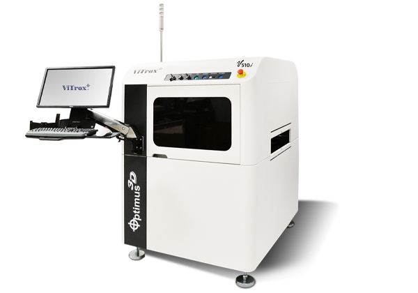
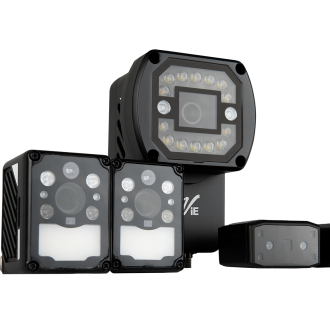
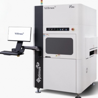
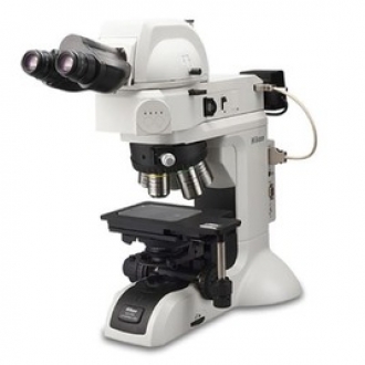
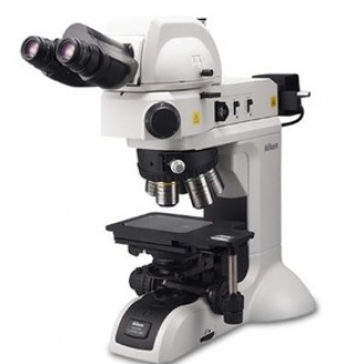
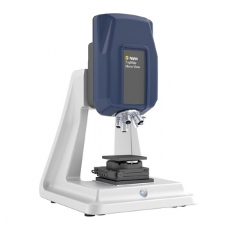
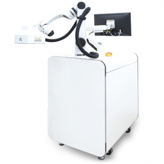
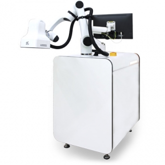
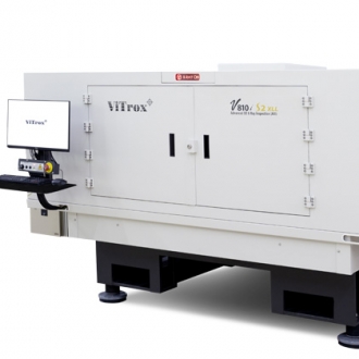
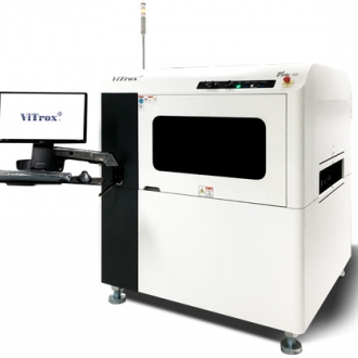
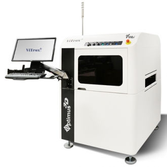
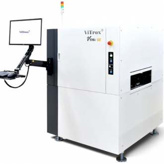
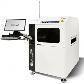
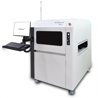
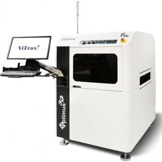
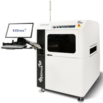
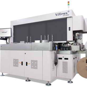
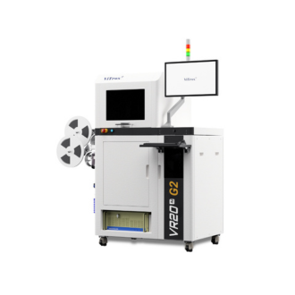
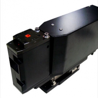
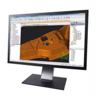
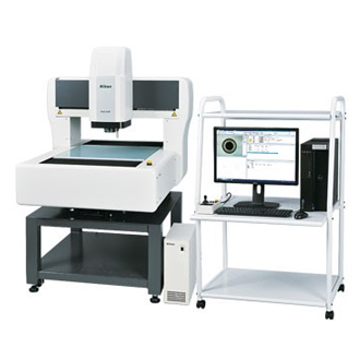
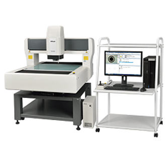
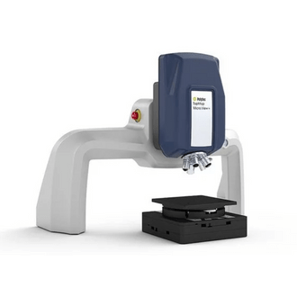
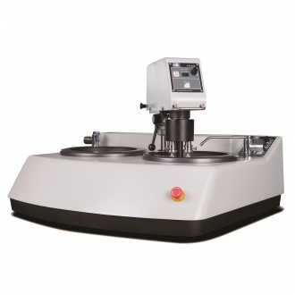
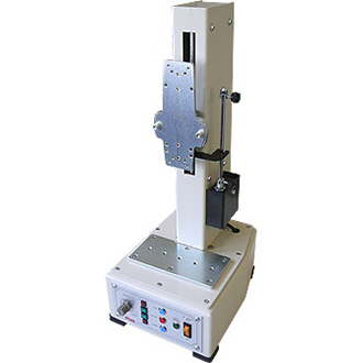
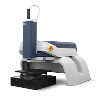
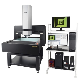
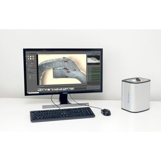
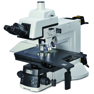
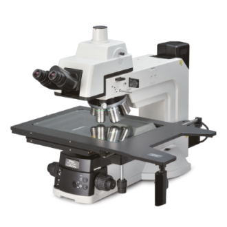
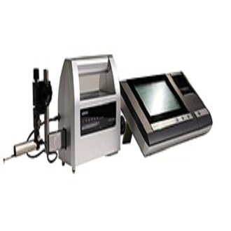
V510i Optimus 3D (for Advanced Packaging and Microelectronics)
| System | AOI for Advanced Packaging | |
| System Performances | ||
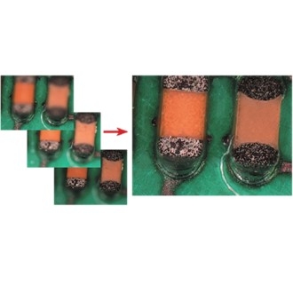
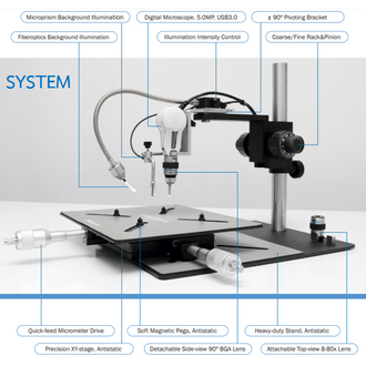
| Component Defect Inspection Categories |
|
|
| Board Level Traceability | Camera-Read Barcodes; External Barcode Reader Configured; OCR Capability with Batch Code Logging | |
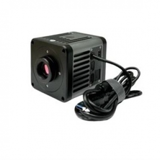
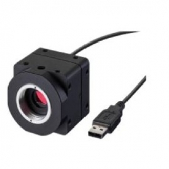
| System Hardware | 12MP | 25MP |
| Operating System | Windows 10 (64-bit) | |
| Optical Resolution & FOV Size | 40mmx30mm @ 10μm telecentric lens 32mmx24mm @ 8µm telecentric lens |
22.5mmx22.5mm @ 4.5μm telecentric lens |
| Inspection Speed | 12MP CoaXPress @ 10μm resolution: 28-42cm²/sec 12MP CoaXPress @ 8μm resolution: 18-26cm²/sec |
25MP CoaXPress @ 4.5μm resolution: 7-15cm²/sec |
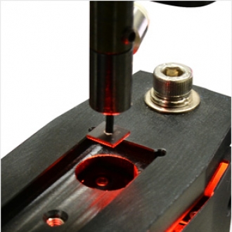
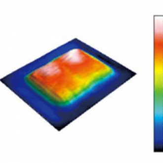
| 3D Technologies | True 3D Inspection with Phase Shift Profilometry’s (PSP) Methodology with 4-way projectors | |
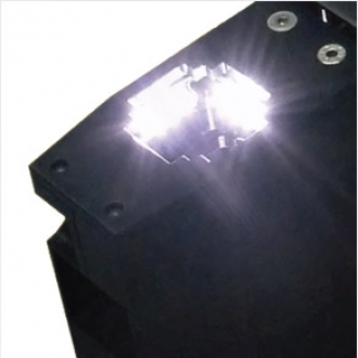
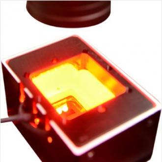
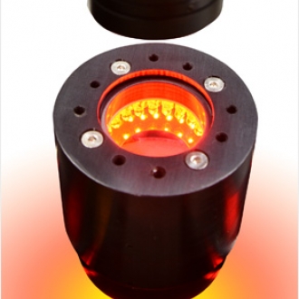
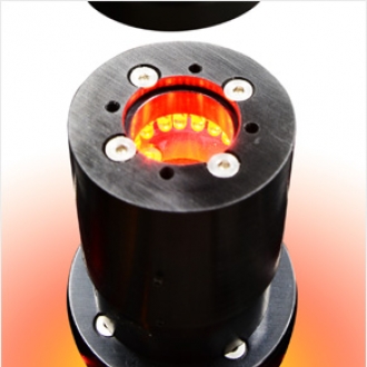
| Lighting Module | Built-in Coaxial Lighting Module, Multiple Color, Multiple Angle, Multiple Segment LED Lighting Head, Auto Calibration Concurrent Lighting Module | |
| Conveyor Width Adjustment | Auto Width Adjustment; Bottom-Up Clamping; In-line SMEMA | Auto Width Adjustment; Bottom-Up Clamping; In-line SMEMA |
| Board Dimension | ||
| Maximum Board Size (L x W) | 490mmx510mm (19.2"x20") | 470mmx500mm (18.5"x19.6") |
| Minimum Board Size (L x W) | 50mmx50mm (2"x2") | 50mmx50mm (2"x2") |
| Maximum Board Thickness | 4mm (0.15") | 4mm (0.15") |
| Minimum Board Thickness | 0.2mm (0.00787") | 0.2mm (0.00787") |
| Maximum PCB Weight | 3kg | 3kg |
| Top Clearance of PCB | 35mm | 10mm |
| Bottom clearance of PCB | 70mm | 70mm |
| PCB Edge Clearance | 3.5mm | 3.5mm |
| PCB Transport Height | 875mm-965mm | 875mm-965mm |
| PCB Temperature | Ambient operating temperature is ~5⁰C to 40⁰C, maximum PCB temperature 80⁰C. | |
* Based on system configuration
Specifications are subject to change.
Related Products
-
 New
NewV510Ai Vision Pro
-
 New
NewV810Ai QX1 Smart 3D AXI System
-
 New
NewViTrox Smart Camera (XC330 Ser…
-
 New
NewLV150NA LED
-
 New
NewF40s
-
 New
NewPixit Zoom
-
 Hot
HotMC4K-Pro
-
 New
NewMA200 LED
-
 New
NewLV150N LED
-
 New
NewH120 – High-Resolution Handhel…
-
 New
NewSLK25 Laser Scanner – High Acc…
-
 New
NewXC65Dx – Cross Laser Scanner f…
-
 New
NewLC15Dx – The Highest-Accuracy …
-
 New
NewL100NX CMM Laser Scanner
-
 New
NewDigital Sight DS-100
-
 New
NewFM-LXR
-
 New
NewOPT SmartFlash-3020
-
 New
NewDigital Microscope Inspectis U…
-
 New
NewViTrox Smart Code Reader (XS S…
-
 New
NewViTrox Smart Camera (XC100 Ser…
-
 New
NewV510Ai DST
-
 New
NewV510Ai ST
-
 New
NewPX730i : Die Sorting & Vision …
-
 New
NewWiX AI: Wafer Vision Inspectio…
-
 New
NewV510Ai AOI for Advanced Packag…
-
 New
NewECLIPSE LV100N POL LED
-
 New
NewLV100NDA LED
-
 New
NewLV100ND LED
-
 Hot
HotMD830M-C Digital Camera
-
 New
NewMD830-C Digital Camera
-
 New
NewMC2000 Digital Camera
-
 New
NewMC500 Digital Camera
-
 New
NewJX 2000 All-in-one Microscope …
-
 New
NewDigital Sight DS-50M
-
 New
NewDigital Sight DS-10
-
 New
NewV510Ai R 6-AXIS
-
 New
NewTMS2400 C Micro.View+ Compact
-
 New
NewNEXIV VMZ-NWL200
-
HANDYSURF+
-
3R-JFIBER Movable tip industri…
-
Inspectis U30S
-
 Hot
HotSMZ25 and SMZ18 Stereo zoom mi…
-
 New
NewV9Ai Final Inspection (FI)
-
 New
NewV9Ai Coating Inspection (CI)
-
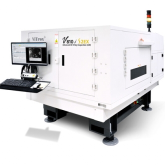
V810Ai S2EX
-
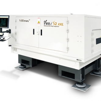
V810Ai S2 XXL
-
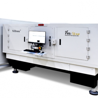
V810Ai S2 XLW
-
V810Ai S2 XLT
-
V810Ai S2 XLL
-
 New
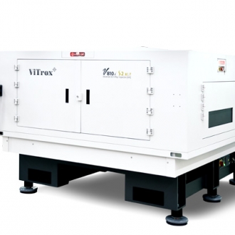
NewV810Ai S3
-
V510Ai DUO
-
V510Ai XXL
-
V510Ai 4.0A
-
V510Ai XLW
-
V510Ai XL
-
V510Ai Optimus 3D
-
 New
NewV510i SE
-
 New
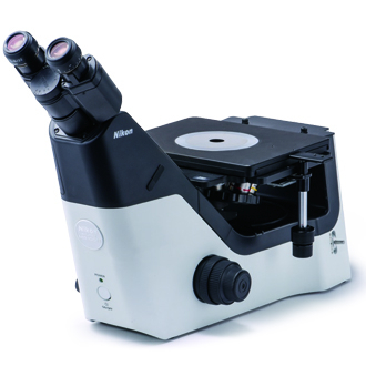
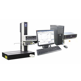
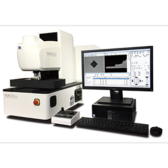
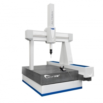
NewV510i Optimus 3D (for Advanced…
-
V310Ai SE
-
V310Ai XXL
-
V310Ai XL
-
V310Ai Optimus
-
 New
NewV310Ai Optimus (for Advanced P…
-
 New
NewTR1000SAi
-
 New
NewTR3000Ai
-
 New
NewTH3000Ai
-
 New
NewVR20Ai L PRO : Post Seal Visio…
-
 New
NewVR20Ai PRO
-
 New
NewVR20Ai G2 : Post Seal Vision H…
-
 New
NewBottom Carrier Tape Inspection
-
 New
NewTape Seal Inspection
-
 New
NewIn-Pocket Inspection
-
 New
New3D & 5 Sided Inspection
-
 New
NewMark, Lead & Package Inspectio…
-
 New
NewOrientation Inspection
-
 Hot
HotNEXIV VMZ-S3020
-
 Hot
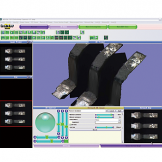
HotEDF/Stitching Express - Softwa…
-
 Hot
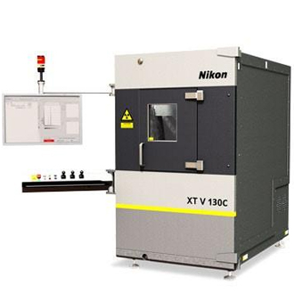
HotXT V 130C
-
 Hot
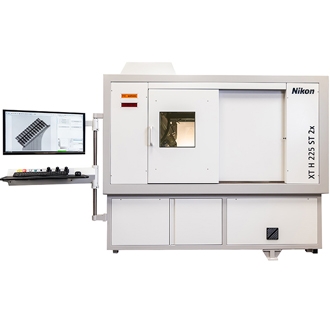
HotXT H 225 | Computed Tomography…
-
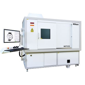
MCT225
-
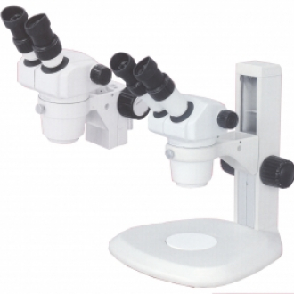
SMZ445 & SMZ460 Stereoscopic Z…
-
 Hot
HotEclipse MA100N
-
Fiber Composite Material Analy…
-

The Extended Porosity/Inclusio…
-
 New
NewTmetric C20 3D camera
-
MAXIMA
-
CMM - CAMIO Software
-
 Hot
HotNEXIV VMZ-S4540
-
 Hot
HotNEXIV VMZ-S6555
-
 Hot
HotiNEXIV VMA-2520
-
 Hot
HotiNEXIV VMA-4540
-
 Hot
HotiNEXIV VMA-6555
-
 New
NewMountain Map - Software
-
 New
New3D CAD Converter - Software
-
 New
NewMapMeasure Pro - Software
-
 New
NewImageFit QC- Software
-
Custom Fit - Software
-
PolyWorks | Modeler
-
 New
NewPolyWorks | ReportLoop
-

PolyWorks | AR
-
 Hot
HotNIS Software
-
 Hot
HotMeasuring Microscope (MM-400)
-
 Hot
HotMeasuring Microscope (MM-800)
-
 Hot
HotE-Max software (DS-Type )
-
 New
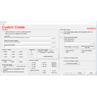
NewCustom Create
-
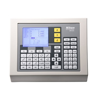
Data Processor (DP-E1A)
-
 New
NewPolyWorks | PMI+Loop
-

PolyWorks | Talisman
-

PolyWorks | DataLoop
-

The Simple Solution for the Vi…
-
V-12B - 12" vertical optical c…
-
 Hot
HotExtended Depth of Focus (EDF) …
-
 Hot
HotTMS 2400
-
 Hot
HotPolyWorks | Inspector
-
 Hot
HotTMS 1400
-
 New
NewSURFCOM NEX
-
SURFCOM CREST DX/SD
-
CONTOURECORD 1600G
-
Wall Thickness analysis with V…
-
FM Series
-
FV Series
-
FLV Series
-
FT-ZERO ARS-F SYSTEM
-
 New
NewFR-XA
-
FR-X Series
-
LC-200R Series
-
FB-3000LC
-
 New
NewFTC-AS Series
-
 New
NewFTC-ASL Series
-

FTC-B255FS
-
FTC-D150A
-
 New
NewFTM-AX
-
FTM-EVO
-
FTP-1AH
-
 New
NewFTP-AX Series
-
 New
NewFTP-MX Series
-
CUTTING WHEEL
-
HOT MOUNTING COMPOUNDS
-
SILICON CABIDE ABRASIVE PAPERS
-
EZ-DISK and MANETIC BASE FOR S…
-

WATER BASE DIAMOND SLURRIES, M…
-

HIGH PURITY ALUMINA (99.9%) an…
-
POLISHING CLOTHS
-
Photonic Fiber Optics Illumina…
-
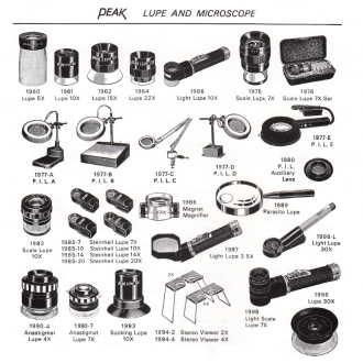
Loupe
-
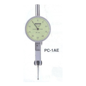
Dial Test Indicators
-
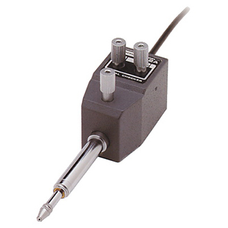
Signal Gauge SC-2A
-
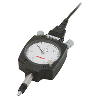
Signal Gauge S-9
-
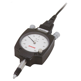
Signal Gauge S-7
-
Signal Gauge S-5
-
DIGITAL GAUGES -D/DL type
-
DIGITAL GAUGES -PND Type
-
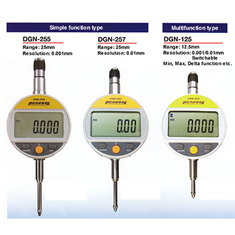
DIGITAL GAUGES -DG type
-
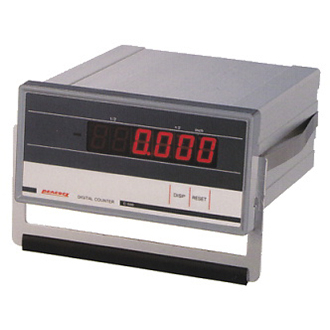
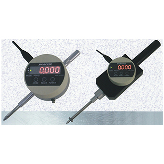
Digital Counters
-
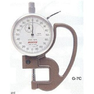
Dial Thickness Gauges
-
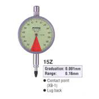
Dial Indicators
-
DIAL GAUGE STANDS & MAGNETIC S…
-
CALIPER GUAGE
-
HAYASHI_Korin KDR6142
-
HAYASHI LP-120 + HDR61WJ
-
TESTING STAND_M Series
-
TESTING STAND_K Series
-
TESTING STAND_KS-504H
-
TESTING STAND_KS-501H
-
TESTING STAND_KS-501E
-
PUSH-PULL GAUGES_MPC series
-
PUSH-PULL GAUGES_MPL series
-
PUSH-PULL GAUGES_MPS series
-
PUSH-PULL GAUGES_MP series
-
PUSH-PULL GAUGES_AP series
-
DIGITAL TORUGE CHECKER_DTC SER…
-
DIGITAL TORUGE CHECKER_ADT-C S…
-
DIGITAL FORCE GUAGES - ARFS SE…
-
DIGITAL FORCE GUAGES - ARF SER…
-
Cylinder Gauges
-
 New
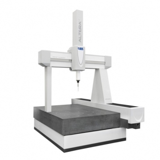
NewALTERA C
-
 Hot
HotMicrendo Series
-
V20B - Large capacity vertical…
-
 Hot
HotFlexiVision 100
-

Nominal/Actual Comparison with…
-
SMZ745 & SMZ745T Stereoscopic …
-
 Hot
HotFlexilux Universal Borescope S…
-
 Hot
HotFiberscope Series
-
 Hot
HotEzyScope
-
 Hot
HotMotorized Stepper Stage For In…
-
Quadra-Check Series
-
 Hot
HotMotorised Stepper Stage For Up…
-
 Hot
HotPro Scan lll
-
Large Sample Non Contact Profi…
-
 Hot
HotNon Contact Flatness Measureme…
-
 Hot
HotNon Contact Flatness Measureme…
-
RONDCOM NEX Rs α
-

PolyWorks | Reviewer
-
 Hot
HotEclipse MA200
-
 Hot
HotVGStudioMax Software
-
 New
NewDigital Sight 1000
-
The Free Viewer App for Your 3…
-
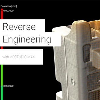
Reverse Engineering with VGStu…
-

Coordinate Measurement Module …
-
 New
NewNew X-ray CT system with enhan…
-
 Hot
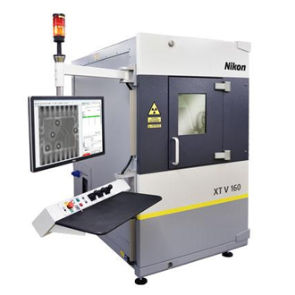
HotXT V 160
-
 Hot
HotE-MAX D Type
-
 Hot
HotStereo Microscope (Paralell) S…
-
 New
NewNEXIV VMF-K6555
-
NEXIV VMZ-H3030
-
 Hot
HotALTERA S
-
SMZ-2 Stereoscopic Zoom Micros…
-
 Hot
HotPorosity/Inclusion Analysis wi…
-
SCANTEK5
-
 Hot
HotData processor (DP-E1A)
-
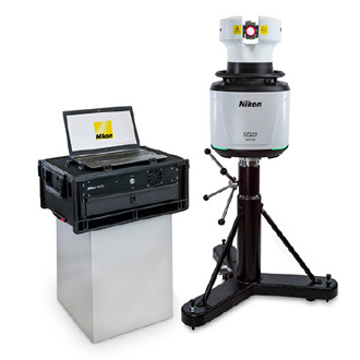
APDIS MV4x0 Laser Radar
-
 Hot
HotALTERA M
-
 New
NewWELDinspect 4K
-
 New
NewBGA Inspection System
-
Digimicro MF-501
-
 Hot
HotEclipse LV150N
-
Eclipse LV100ND
-
Eclipse LV100N POL
-
Eclipse L200N Series
-
Eclipse L300N Series
-
Digimicro MF-1001
-
 Hot
HotNEXIV AutoMeasure Software
-
 New
NewCMM-Manager for iNEXIV Softwar…
-
DIGITAL FORCE GUAGES - ARF ser…
-
 New
NewNEXIV Remote Control SDK
-
TOUCH50
-
ALTERA SL
-
 New
NewNEXIV VMF-K3020