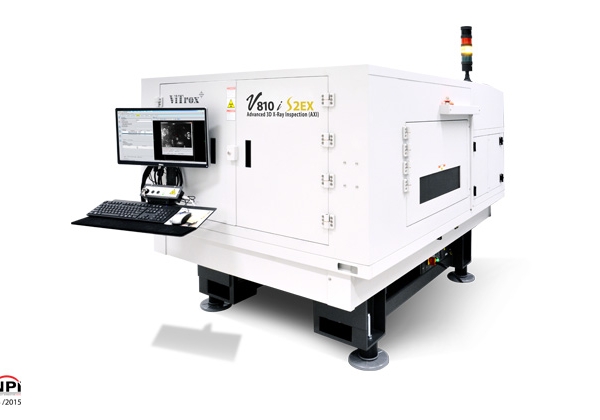

V810i S2EX
| System | V810i S2 Series | |
| System controller | Integrated controller with 8 Core Intel Xeon processors | |
| Operating system | Windows 10 Pro (64 bit) | |
| Test Development Environment | ||
| User interface | Microsoft Windows based software solution with easy-to-use GUI and password-protected user levels | |
| Off-line test development software | Optional for off-line PC | |
| CAD conversion tool | Support 4 different types of CAD in V810i software and optional software available to translate other CAD data to ViTrox's format | |
| Typical test development time | 4 hours to 1.5 days to convert raw CAD file and develop application | |
| Line Integration | ||
| Transport heights | 865mm-1025mm | |
| Line communication standard | SMEMA, HERMES | |
| Barcode readers | Compatible with most industry standard barcode readers | |
| Performance Parameters* | ||
| False Call rate | 500-1000ppm | |
| Minimum features detection capability | ||
| Joint pitch1 | 0.3mm and above | |
| Short width2 | 0.045mm | |
| Solder thickness | 0.0127mm | |
| Allowable Panel Characteristics ** | Standard | DL |
| Maximum PCB Size (L x W) | 609.6mmx482.6mm (24"x19") | Dual Lane: 457mmx206mm (18"x8.1") Single Lane: 457mmx400mm (18"x15.7") |
| Minimum PCB Size (L x W) | 76.2mmx76.2mm (3"x3") | 76mmx101.6mm (3"x4") |
| Maximum PCB inspectable area | 609.6mmx474.9mm (24"x18.7") | Dual Lane: 457mmx198.1mm (18"x7.8") Single Lane: 457mmx391.1mm (18"x15.4") (Not supported longboard scanning) |
| Maximum PCB thickness | 7mm (275 mils) | 5mm (196mils) |
| Minimum PCB thickness | 0.5mm (20 mils) | |
| PCB warp | Downside < 3.3mm; Upside < 1.5mm | |
| Maximum PCB weight | 4.5kg | |
| Top Clearance of PCB | 50mm @ 23µm resolution 38mm @ 19µm resolution 38mm @ 10.5µm resolution# 11mm @ 11µm resolution 11mm @ 6µm resolution# (Calculated from Board Top surface) |
|
| Bottom Clearance of PCB | 70mm | 60mm |
| PCB edge clearance | 3mm | |
| 100% Press-fit testability | Yes (With PSP2 / PSP2.1 feature) | |
| PCB Temperature | 40℃ | |
| Installation Specification | ||
| Power Supplies | 200–240 VAC three phase; 380–415 VAC three phase wye (+/- 5) (50Hz or 60Hz) | |
| Air requirement | 552kPA (80psi) | |
| System footprint (Width X Depth X Height) | 1566mmx2145mmx1972mm | |
| Total system weight | ~3800kgs | |
| **Note: 1. Panels are handled on width edges. Panels with edge cut outs may require the use of a carrier. 2. Maximum panel size dimensions and weight must include carrier if applicable 3. Smaller panels are possible with the use of panel carriers. 4. With panels of this thickness, imaging results can be affected by PCBA layout. 5. Measured from the bottom of the panel including a maximum warp. *Note: 1. Assuming pad width is 50% of pitch. 2. The reported values for minimum feature detection assume that the feature is in a single plane of focus and that there are no X-ray absorbers in the X-ray path or in the immediate area of the feature other than those found in a typical multi-layer printed circuit board. #2x2 binning camera configuration. Hardware upgrade is required on old system. |
||
Related Products
-
New
MA200 LED
-
New
LV150N LED
-
 New
NewH120 – สแกนเนอร์เลเซอร์ 3 มิติ…
-
 New
NewSLK25 Laser Scanner – ความแม่น…
-
 New
NewXC65Dx – เลเซอร์ครอสสแกนเนอร์ส…
-
 New
NewLC15Dx – เลเซอร์สแกนเนอร์ความแ…
-
 New
NewL100NX CMM Laser Scanner
-
New
Digital Sight DS-100
-
 New
NewFM-LXR
-
 New
NewOPT SmartFlash 3020
-
 New
NewDigital Microscope Inspectis U…
-
 New
NewViTrox Smart Code Reader (XS S…
-
 New
NewViTrox Smart Camera (XC Series…
-
 New
NewV510i DST
-
 New
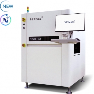
NewV510i ST
-
 New
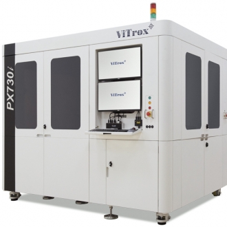
NewPX730i : Die Sorting & Vision …
-
 New
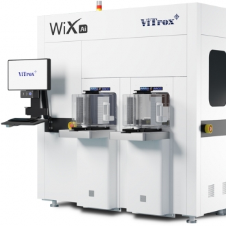
NewWiX AI: เครื่องตรวจสอบเวเฟอร์ด…
-
 New
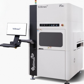
NewV510i AOI for Advanced Packagi…
-
 New
NewECLIPSE LV100N POL LED
-
 New
NewLV100NDA LED
-
 New
NewLV100ND LED
-
 Hot
HotMD830M-C Digital Camera
-
 New
NewMD830-C Digital Camera
-
 New
NewMC2000 Digital Camera
-
 New
NewMC500 Digital Camera
-
 New
NewJX 2000 All-in-one Microscope …
-
 New
NewDigital Sight DS-50M
-
 New
NewDigital Sight DS-10
-
 New
Newวิวัฒนาการใหม่ของการเคลือบตามแ…
-
New
TMS2400 C Micro.View+ Compact
-
 New
NewNEXIV VMZ-NWL200
-
HANDYSURF+--
-
3R-JFIBER Movable tip industri…
-
Inspectis U30S
-
 Hot
HotSMZ25 and SMZ18 Stereo zoom mi…
-
 New
NewV9i Final Inspection (FI)
-
 New
NewV9i Coating Inspection (CI)
-
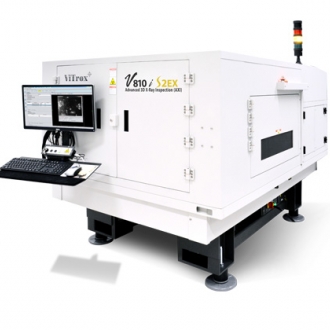
V810i S2EX
-
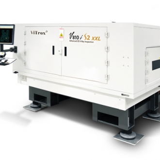
V810i S2 XXL
-
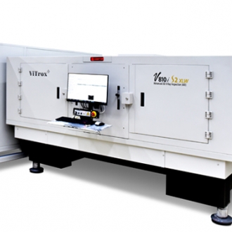
V810i S2 XLW
-
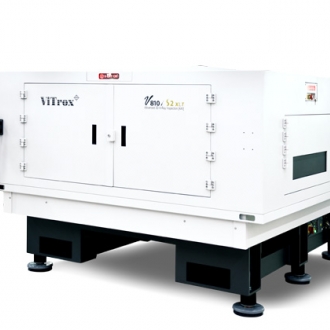
V810i S2 XLT
-
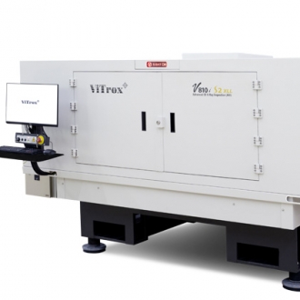
V810i S2 XLL
-
 New
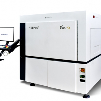
NewV810i S3
-
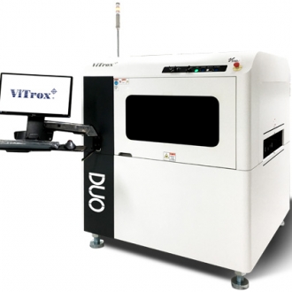
V510i DUO
-
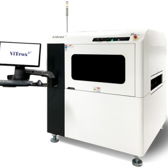
V510i XXL
-
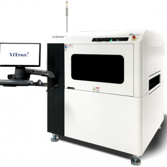
V510i 4.0
-
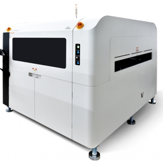
V510i XLW
-
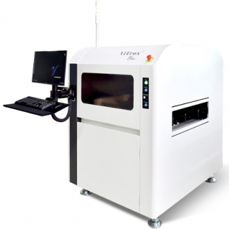
V510i XL
-
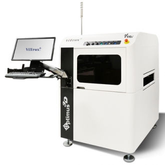
V510i Optimus 3D
-
 New
NewV510i SE
-
 New
NewV510i Optimus 3D (for Advanced…
-
V310i SE
-
V310i XXL
-
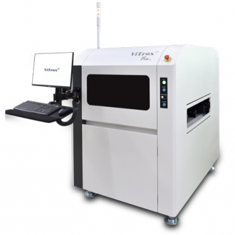
V310i XL
-
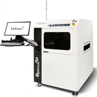
V310i
-
 New
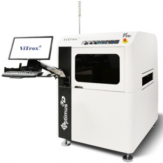
NewV310i Optimus (for Advanced Pa…
-
 New
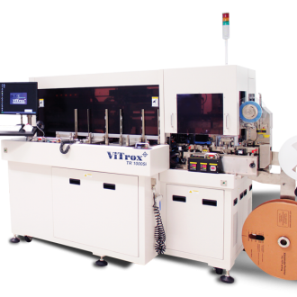
NewTR1000Si
-
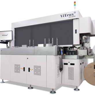 New
NewTR3000i
-
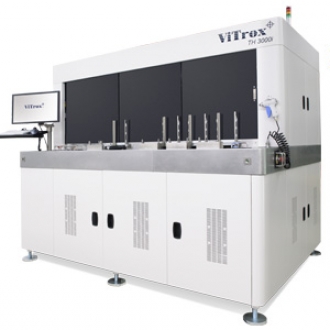 New
NewTH3000i
-
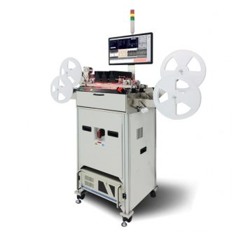 New
NewVR20 Li
-
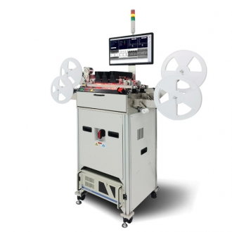 New
NewVR20 i
-
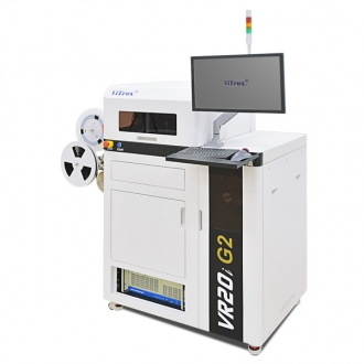 New
NewVR20i G2
-
 New
Newกล้องตรวจสอบเทปด้านล่าง
-
 New
Newกล้องตรวจสอบซีลเทป
-
 New
Newกล้องตรวจสอบวัตถุในพ๊อกเก็ต
-
 New
Newกล้องตรวจสอบ 3 มิติและ 5 ด้าน
-
 New
Newกล้องตรวจสอบเครื่องหมาย ขางานแ…
-
 New
Newกล้องตรวจสอบทิศทาง
-
 Hot
HotNEXIV VMZ-S3020
-
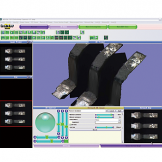 Hot
HotEDF/Stitching Express - Softwa…
-
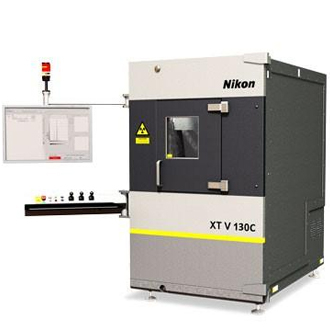 Hot
HotXT V 130C
-
 Hot
HotXT H 225 | Computed Tomography…
-
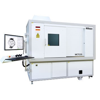
MCT225
-
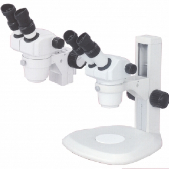
SMZ445 & SMZ460 Stereoscopic Z…
-
 Hot
HotEclipse MA100N
-
Fiber Composite Material Analy…
-

The Extended Porosity/Inclusio…
-
 New
NewTmetric C20 3D camera
-
MAXIMA
-
CMM - CAMIO Software
-
 Hot
HotNEXIV VMZ-S4540
-
 Hot
HotNEXIV VMZ-S6555
-
 Hot
HotiNEXIV VMA-2520
-
 Hot
HotiNEXIV VMA-4540
-
 Hot
HotiNEXIV VMA-6555
-
 New
NewMountain Map - Software
-
 New
New3D CAD Converter - Software
-
 New
NewMapMeasure Pro - Software
-
 New
NewImageFit QC- Software
-
Custom Fit - Software
-
PolyWorks | Modeler
-
 New
NewPolyWorks | ReportLoop
-

PolyWorks | AR
-
 Hot
HotNIS Software
-
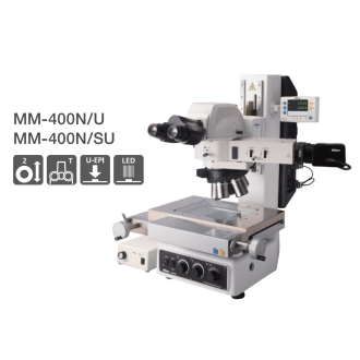 Hot
HotMeasuring Microscope (MM-400)
-
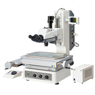 Hot
HotMeasuring Microscope (MM-800)
-
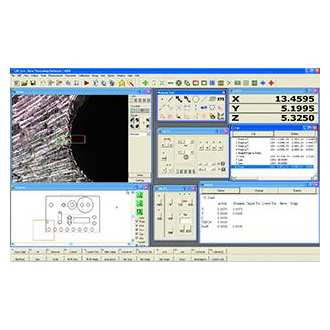 Hot
HotE-Max software (DS-Type )
-
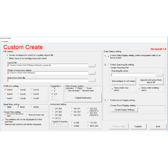 New
NewCustom Create
-
Data Processor (DP-E1A)
-
 New
NewPolyWorks | PMI+Loop
-

PolyWorks | Talisman
-

PolyWorks | DataLoop
-

The Simple Solution for the Vi…
-
V-12B - 12" vertical optical c…
-
 Hot
HotExtended Depth of Focus (EDF) …
-
 Hot
HotTMS 2400
-
 Hot
HotPolyWorks | Inspector
-
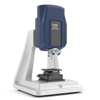 Hot
HotTMS 1400
-
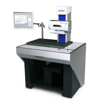 New
NewSURFCOM NEX
-
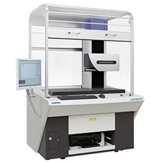
SURFCOM CREST DX/SD
-
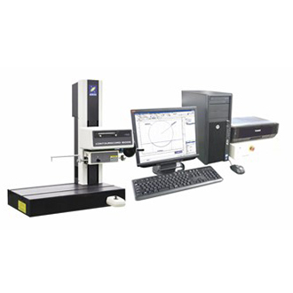
CONTOURECORD 1600G
-
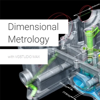
Wall Thickness analysis with V…
-
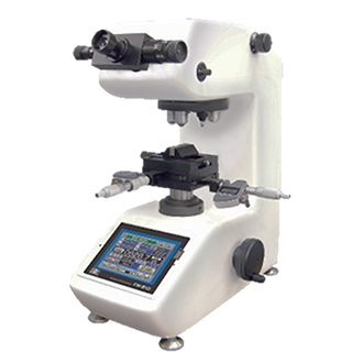
FM Series
-
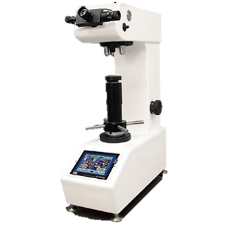
FV Series
-
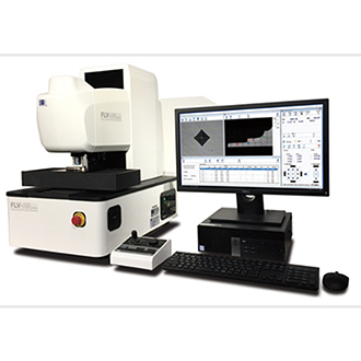
FLV Series
-
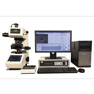
FT-ZERO ARS-F SYSTEM
-
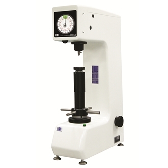 New
NewFR-XA
-
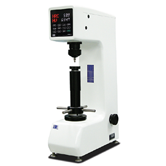
FR-X Series
-
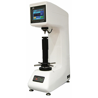
LC-200R Series
-
FB-3000LC
-
 New
NewFTC-AS Series
-
 New
NewFTC-ASL Series
-

FTC-B255FS
-
FTC-D150A
-
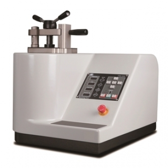 New
NewFTM-AX
-
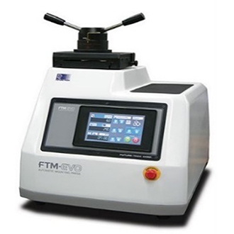
FTM-EVO
-
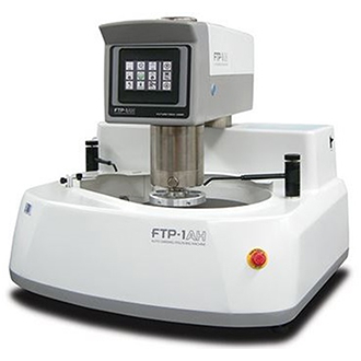
FTP-1AH
-
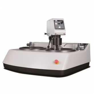 New
NewFTP-AX Series
-
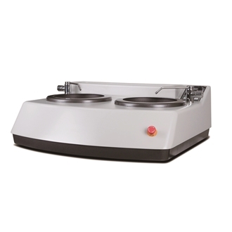 New
NewFTP-MX Series
-
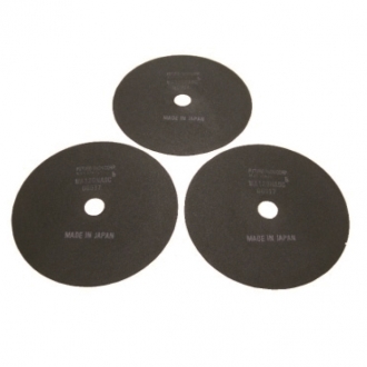
CUTTING WHEEL
-
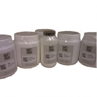
HOT MOUNTING COMPOUNDS
-
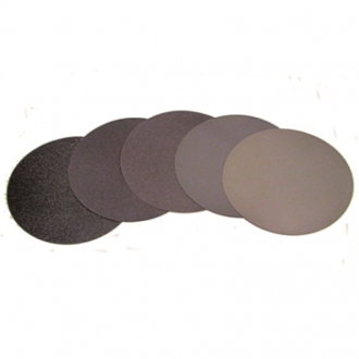
SILICON CABIDE ABRASIVE PAPERS
-
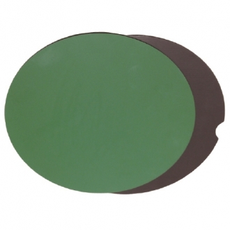
EZ-DISK and MANETIC BASE FOR S…
-

WATER BASE DIAMOND SLURRIES, M…
-
HIGH PURITY ALUMINA (99.9%) an…
-
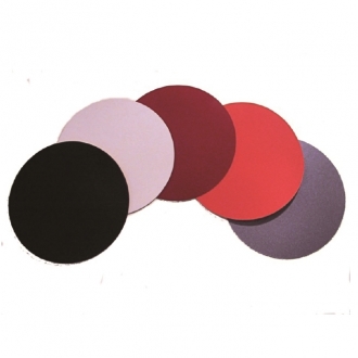
POLISHING CLOTHS
-
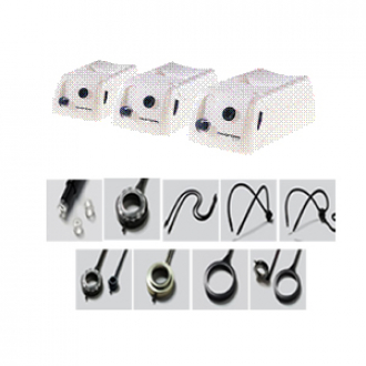
Photonic Fiber Optics Illumina…
-
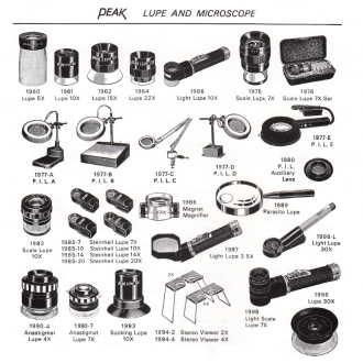
Loupe
-
Dial Test Indicators
-
Signal Gauge SC-2A
-
Signal Gauge S-9
-
Signal Gauge S-7
-
Signal Gauge S-5
-
DIGITAL GAUGES -D/DL type
-
DIGITAL GAUGES -PND Type
-
DIGITAL GAUGES -DG type
-
Digital Counters
-
Dial Thickness Gauges
-
Dial Indicators
-
DIAL GAUGE STANDS & MAGNETIC S…
-
CALIPER GUAGE
-
HAYASHI_Korin KDR6142
-
HAYASHI LP-120 + HDR61WJ
-
TESTING STAND_M Series
-
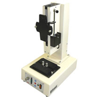
TESTING STAND_K Series
-
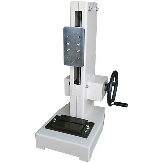
TESTING STAND_KS-504H
-
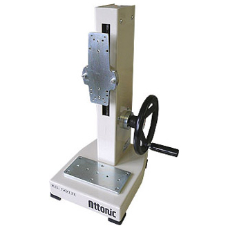
TESTING STAND_KS-501H
-
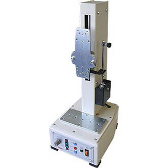
TESTING STAND_KS-501E
-
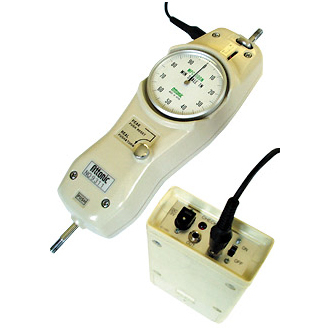
PUSH-PULL GAUGES_MPC series
-
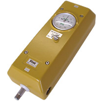
PUSH-PULL GAUGES_MPL series
-
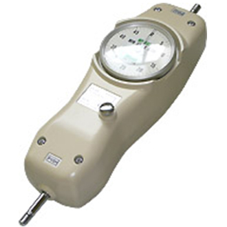
PUSH-PULL GAUGES_MPS series
-
PUSH-PULL GAUGES_MP series
-
PUSH-PULL GAUGES_AP series
-
DIGITAL TORUGE CHECKER_DTC SER…
-
DIGITAL TORUGE CHECKER_ADT-C S…
-
DIGITAL FORCE GUAGES - ARFS SE…
-
DIGITAL FORCE GUAGES - ARF SER…
-
Cylinder Gauges
-
 New
NewALTERA C
-
 Hot
HotMicrendo Series
-
V20B - Large capacity vertical…
-
 Hot
HotFlexiVision 100
-

Nominal/Actual Comparison with…
-
SMZ745 & SMZ745T Stereoscopic …
-
 Hot
HotFlexilux Universal Borescope S…
-
 Hot
HotFiberscope Series
-
 Hot
HotEzyScope
-
 Hot
HotMotorized Stepper Stage For In…
-
Quadra-Check Series
-
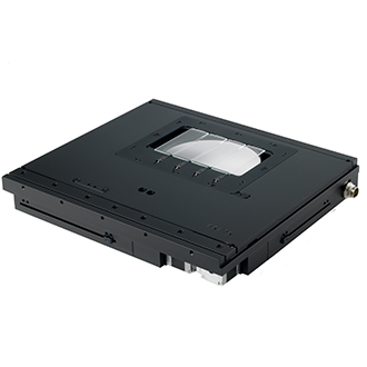 Hot
HotMotorised Stepper Stage For Up…
-
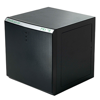 Hot
HotPro Scan lll
-
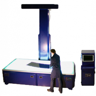
Large Sample Non Contact Profi…
-
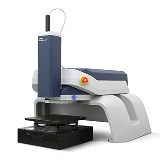 Hot
HotNon Contact Flatness Measureme…
-
 Hot
HotNon Contact Flatness Measureme…
-
RONDCOM NEX Rs α
-

PolyWorks | Reviewer
-
 Hot
HotEclipse MA200
-
 Hot
HotVGStudioMax Software
-
 New
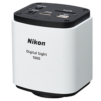
NewDigital Sight 1000
-
The Free Viewer App for Your 3…
-
Reverse Engineering with VGStu…
-

Coordinate Measurement Module …
-
 New
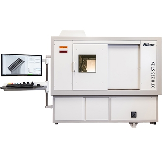
NewNew X-ray CT system with enhan…
-
 Hot
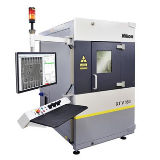
HotXT V 160
-
 Hot
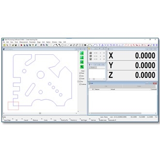
HotE-MAX D Type
-
 Hot
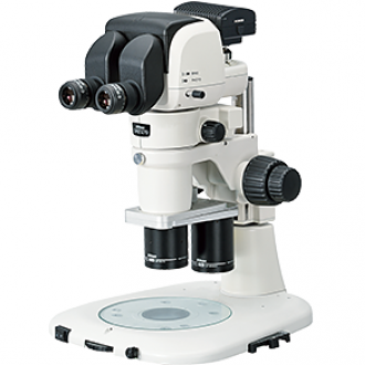
HotStereo Microscope (Paralell) S…
-
 New
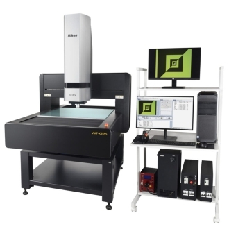
NewNEXIV VMF-K6555
-
NEXIV VMZ-H3030
-
 Hot
HotALTERA S
-
SMZ-2 Stereoscopic Zoom Micros…
-
 Hot
HotPorosity/Inclusion Analysis wi…
-
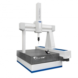
SCANTEK5
-
 Hot
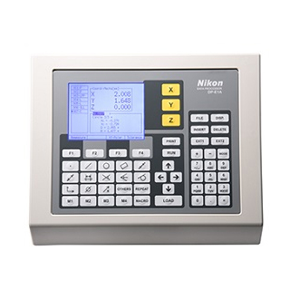
HotData processor (DP-E1A)
-
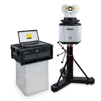
APDIS MV4x0 Laser Radar
-
 Hot
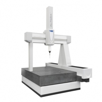
HotALTERA M
-
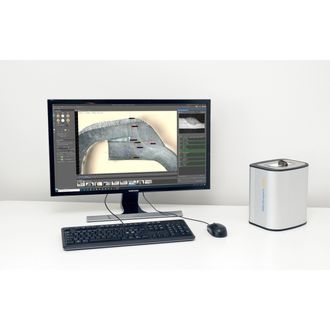 New
NewWELDinspect 4K
-
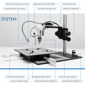 New
NewBGA Inspection System
-
Digimicro MF-501
-
 Hot
HotEclipse LV150N
-
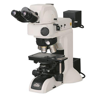
Eclipse LV100ND
-
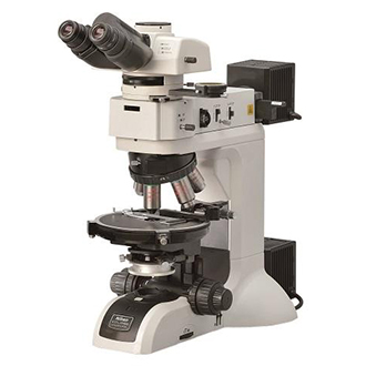
Eclipse LV100N POL
-
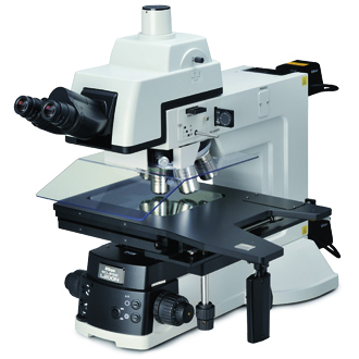
Eclipse L200N Series
-
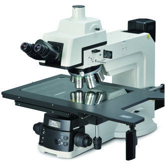
Eclipse L300N Series
-
Digimicro MF-1001
-
 Hot
HotNEXIV AutoMeasure Software
-
 New
NewCMM-Manager for iNEXIV Softwar…
-
DIGITAL FORCE GUAGES - ARF ser…
-
 New
NewNEXIV Remote Control SDK
-
TOUCH50
-
ALTERA SL
-
 New
NewNEXIV VMF-K3020


